


-
Group News2025-03-28
- iSABers SEMICON Moment: Offline Innovation Sharing Session Successfully Held


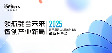
On March 26th, iSABers held an offline technological innovation sharing session themed "Pioneering the Future of Bonding, Innovating a New Landscape for the Industry" during the 2025 SEMICON China, which attracted extensive attention from the semiconductor industry. At the sharing session, iSABers fully demonstrated its latest breakthroughs in the field of high-end bonding equipment.
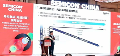
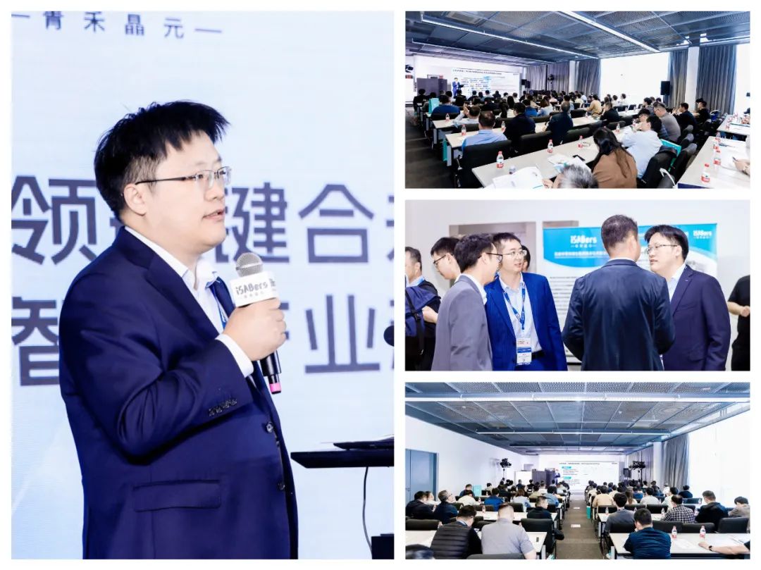 On site sharing session
As a core segment of chip manufacturing, semiconductor bonding technology’s precision and efficiency directly determine chip performance. However, for a long time, the high-end bonding equipment market has been monopolized by overseas enterprises, leaving Chinese semiconductor companies facing challenges such as technological blockades, high costs, and long delivery cycles.
Dr. Mu Fengwen, Founder and Chairman of iSABers, stated at the sharing session: “Facing overseas monopolies, iSABers has firmly chosen independent innovation, breaking industry barriers with core technological breakthroughs to provide efficient and reliable bonding solutions for China's semiconductor industry.”
Over the past five years, iSABers has overcome “necklace-breaking” technologies such as room-temperature bonding and 3D heterogeneous integration, developing four core equipment lines covering cutting-edge fields like advanced packaging and wafer-level integration. In 2024, the company secured over 30 orders annually, with a total value exceeding 300 million yuan, demonstrating remarkable achievements.
The five independently controllable core technologies mastered by the company are the key to its leadership in semiconductor heterogeneous integration:
Surface Activation Bonding: Mastery of full sets of surface activation technologies such as ICPCCPFAB, covering all bonding equipment scenarios;
Submicron Precision Alignment Technology: Mastery of mainstream submicron alignment technologies such as Face-to-Face, inter-chip coaxial, and infrared penetration;
Ultra-High Vacuum Technology: Completing activation, alignment, and other processes in ultra-high vacuum environments to overcome vacuum-related challenges;
Temperature and Pressure Control Bonding Technology: Ensuring uniformity in high-temperature and high-pressure environments;
Single-Wafer Spin Coating/Cleaning Technology: High-speed rotational dynamic balance to prevent backflow contamination and ensure high bonding yield rates.
Relying on these technologies, iSABers has established a dual-driven business model of “R&D and manufacturing of high-end equipment + precision bonding process foundry,” providing comprehensive solutions for the global semiconductor industry chain.
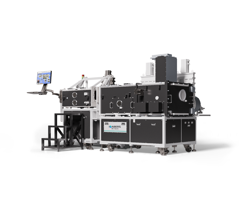
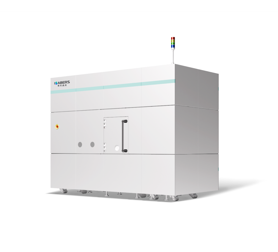
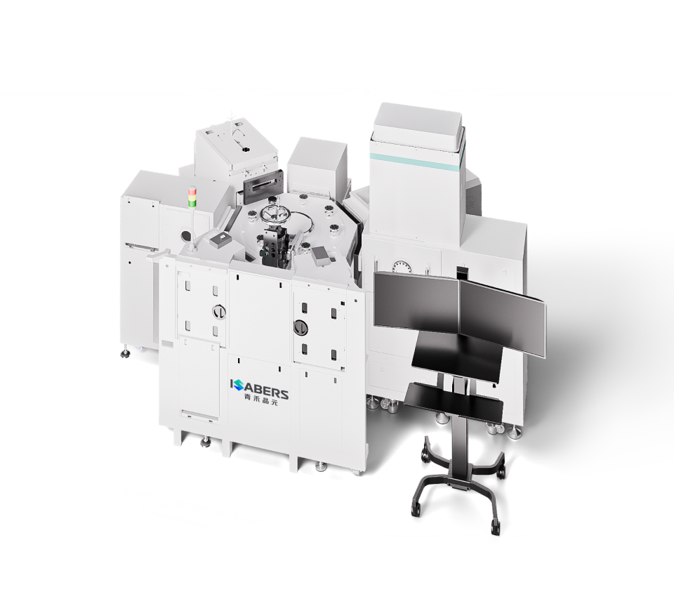
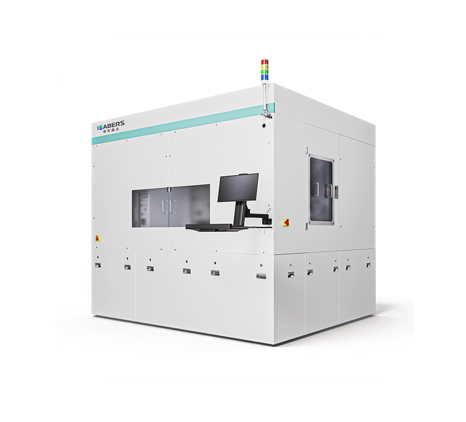
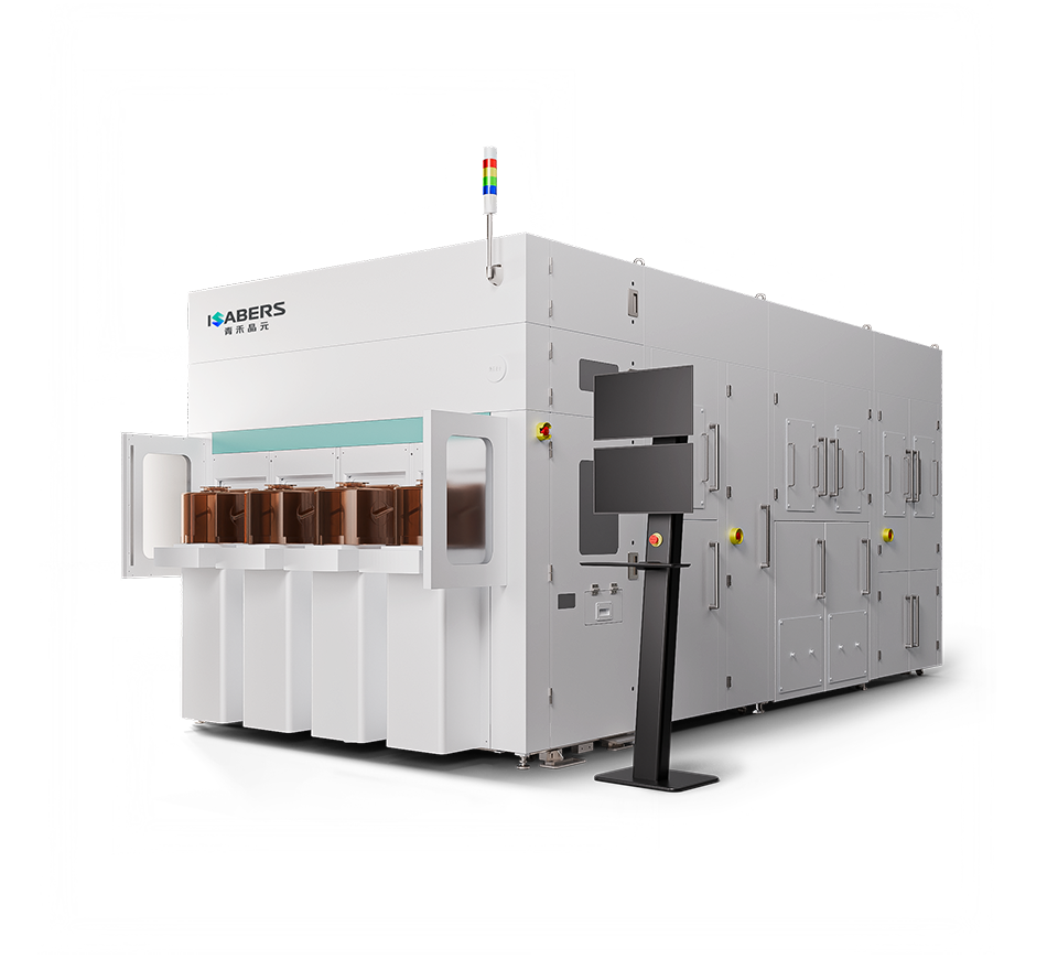
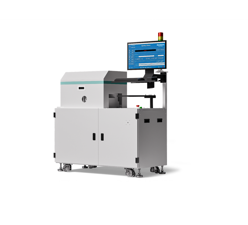
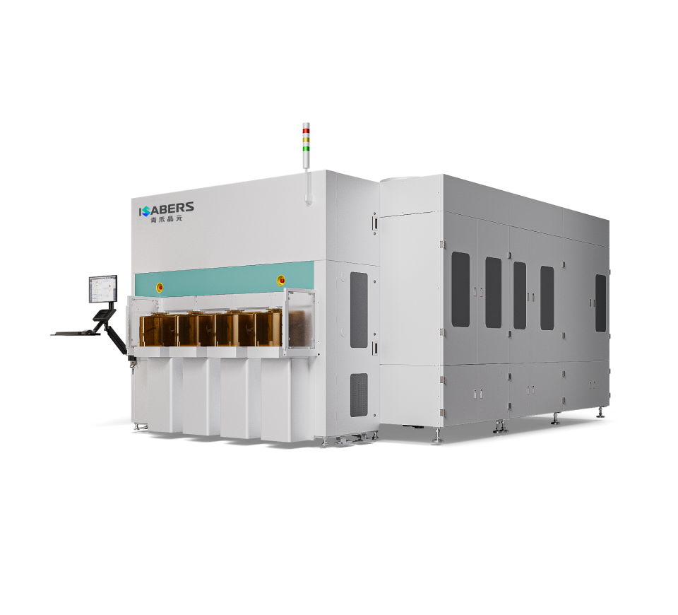
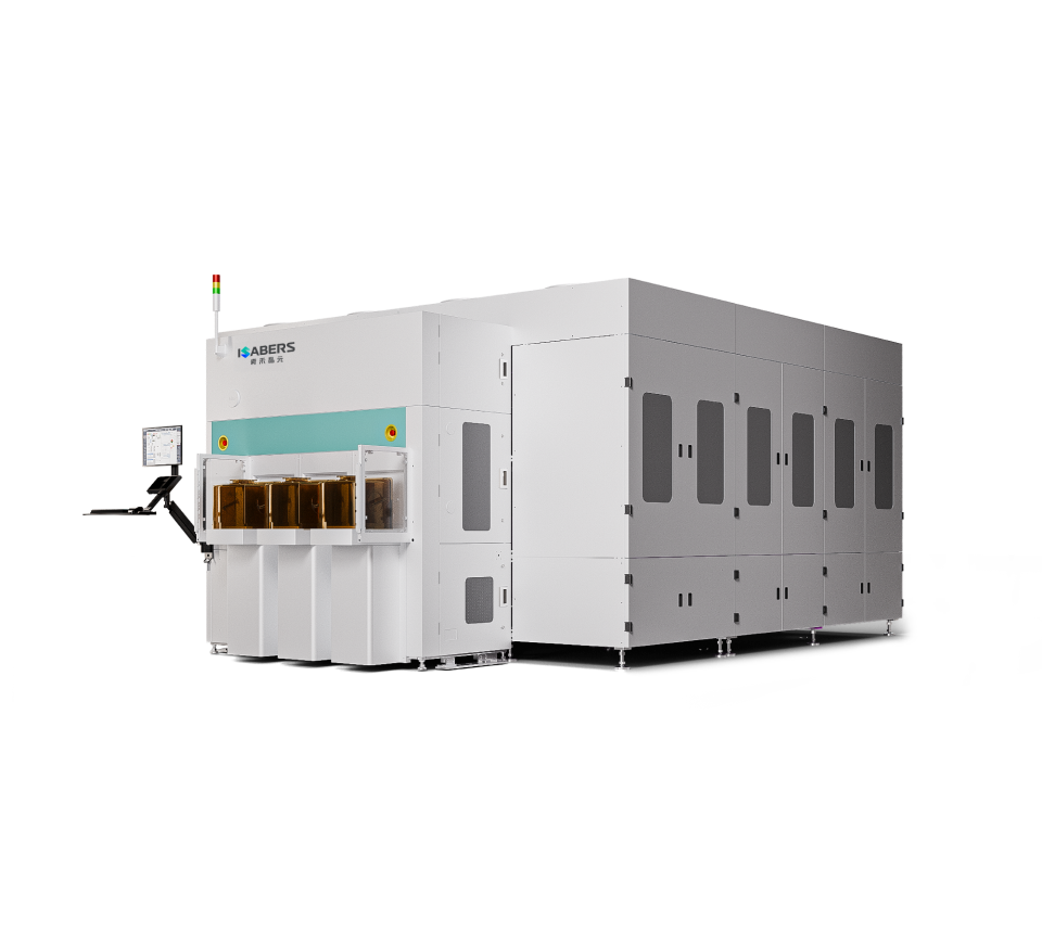
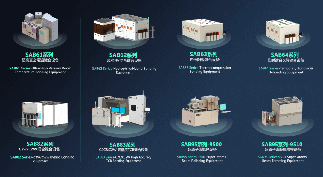
The event showcased a series of technologically leading wafer and chip bonding equipment independently developed by iSABers, including ultra-high vacuum room-temperature bonding, hydrophilic/hybrid bonding, thermocompression/anodic bonding, and temporary bonding&debonding equipment. These devices have attracted enthusiastic attention and in-depth negotiations from industry clients due to their excellent alignment accuracy and broad material compatibility.
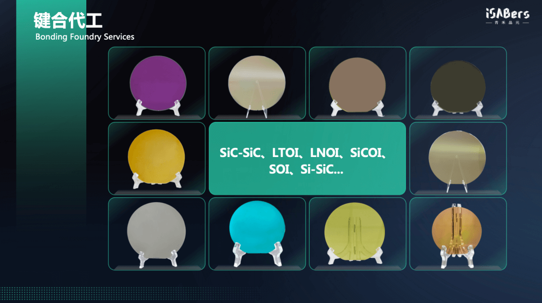
Additionally, iSABers has established modern bonding foundry mass production lines in Tianjin and Shanxi, capable of stably mass-producing various critical bonding substrates while continuously optimizing processes to improve yield rates.
Mu Fengwen stated: “Domestic substitution is just the first step. Our vision is to become a global leader in semiconductor heterogeneous integration. In the future, iSABers will not only bring Chinese technologies to the world stage but also redefine the frontiers of bonding technology through innovation, delivering value beyond expectations to global customers.”
iSABers’ technological breakthroughs signal that the semiconductor bonding technology field is on the cusp of a new era driven by Chinese technology. Through technological innovation, ecological co-construction, and long-term investment, iSABers is gradually realizing its grand vision and pushing China's semiconductor industry to higher levels.
From conquering core processes to building a complete product portfolio, and from technological innovation to ecological co-construction, iSABers has demonstrated deep expertise in semiconductor bonding and the hardcore strength of Chinese enterprises to break through technological blockades. At the 2025 SEMICON China exhibition, iSABers, participating for the first time, showcased the new look of Chinese semiconductor bonding technology to the world, heralding profound changes in the global semiconductor industry landscape.
-
Latest News
- 2025-05-01
- Pay tribute to the strivers in the semiconductor industry and wish you a happy May Day!
-
Latest News
- 2025-04-21
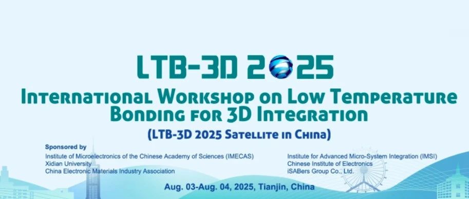
- iSABers Co-hosted – 2025 China International Seminar on Low-Temperature Bonding and 3D Integration Technology Invites You to Participate
-
Latest News
- 2025-03-28
- iSABers SEMICON Moment: Offline Innovation Sharing Session Successfully Held
-
Latest News
- 2025-03-27
- iSABers' SEMICON Moment: Showcasing China's Solutions for Advanced Bonding Technology
-
Latest News
- 2025-03-21
- SEMICON In-Person Advanced Bonding Technology Breakthroughs Symposium