


-
Group News2025-03-27
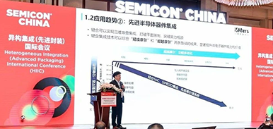
- iSABers' SEMICON Moment: Showcasing China's Solutions for Advanced Bonding Technology


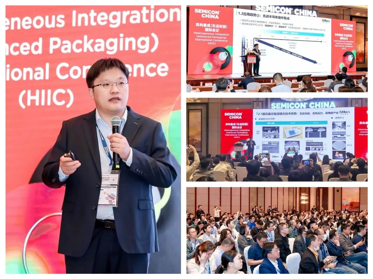 Dr. Mu Fengwen Sharing at the Conference
As one of the core processes in semiconductor manufacturing, bonding technology is propelling the industry into the "third wave of materials technology." In her speech, Dr. Mu emphasized that as Moore's Law approaches its physical limits, achieving performance breakthroughs through heterogeneous material integration and 3D stacking has become a critical development direction for the global semiconductor industry.
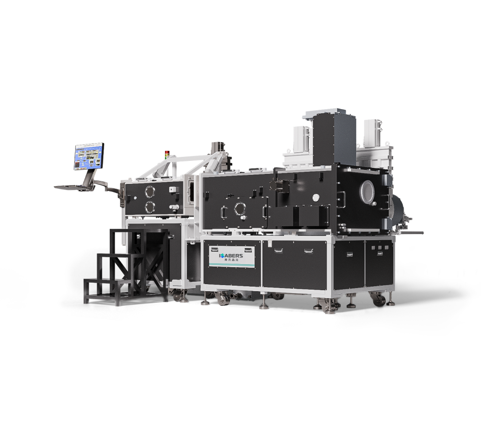
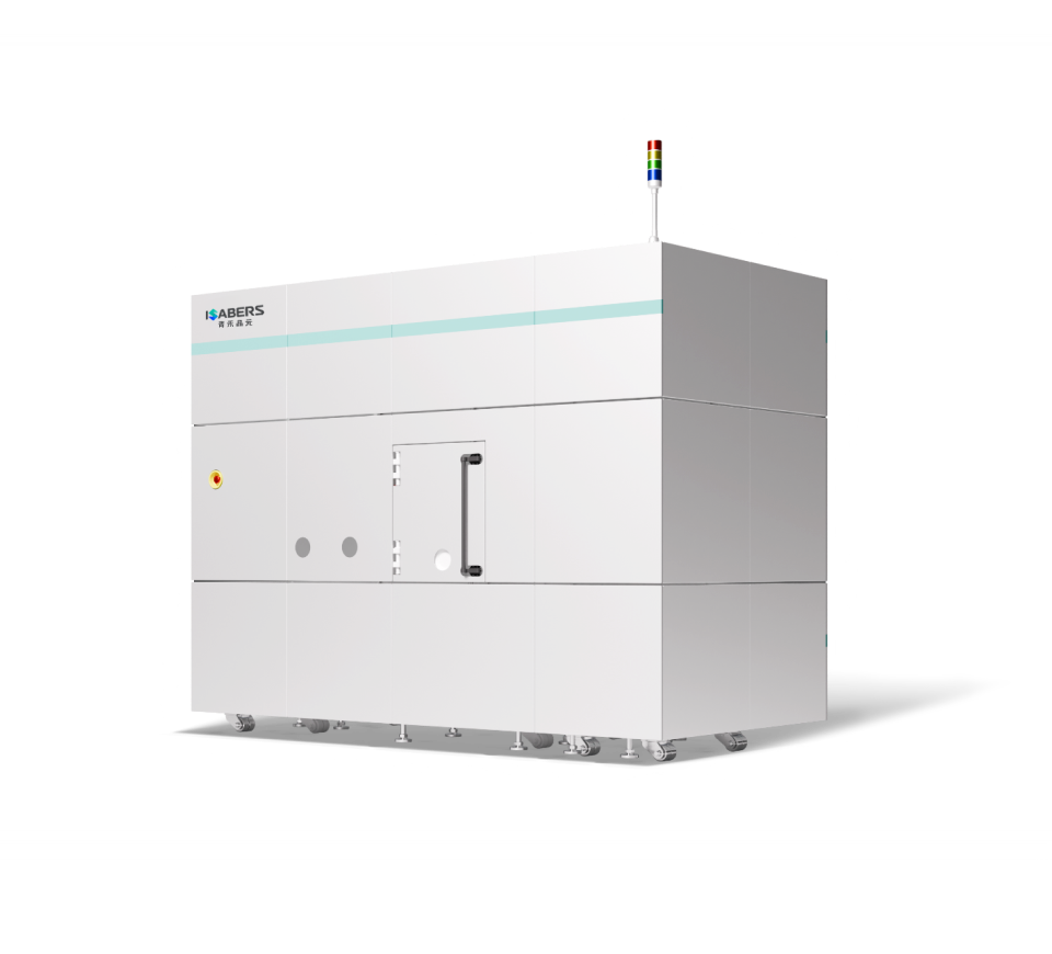
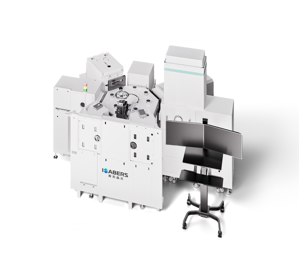
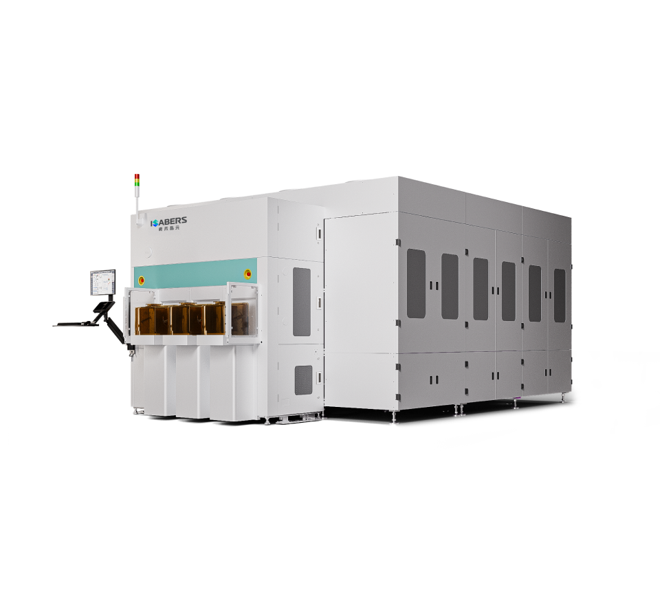
In the technical sharing session, Dr. Mu detailed iSABers' innovative achievements in ultra-high vacuum room-temperature bonding. This breakthrough technology offers significant advantages over traditional methods, including no reaction layer, no temperature cycling, high precision, and high throughput, enabling non-destructive integration of wide-bandgap semiconductor materials such as SiC and GaN. This provides clients with substantial cost advantages.
In the field of 3D integration, Dr. Mu highlighted iSABers' globally first independently developed C2W/W2W dual-mode hybrid bonding equipment. This equipment perfectly addresses the interconnection bottleneck in HBM memory stacking, offering more flexible solutions for 3D IC design. Dr. Mu noted: "To achieve 16-layer DRAM stacking within the 720-micron thickness required for HBM4, hybrid bonding technology must replace traditional bump processes."
In POI substrate foundry services, room-temperature bonding technology has successfully achieved reliable bonding of LT (lithium tantalate) with silicon, sapphire, and other materials, effectively avoiding thermal stress issues. This innovation has provided critical support for 5G RF devices and has been recognized by leading industry clients.
Significant progress has also been made in temporary bonding technology: the inorganic solution can withstand high temperatures of 1000°C with submicron-level thickness control accuracy. Compared to traditional organic solutions, this technology is more suitable for ultra-thin wafer processing in memory devices, CIS, and other applications.
In her concluding remarks, Dr. Mu envisioned the future of bonding technology: "With the explosion of emerging applications such as AI and autonomous driving, demand for heterogeneous integration will grow exponentially. iSABers will continue to increase R&D investments and collaborate with global partners to drive technological innovation in the semiconductor industry."
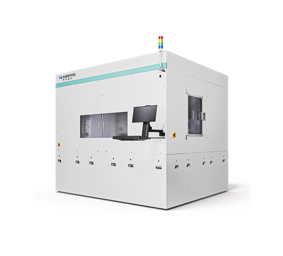
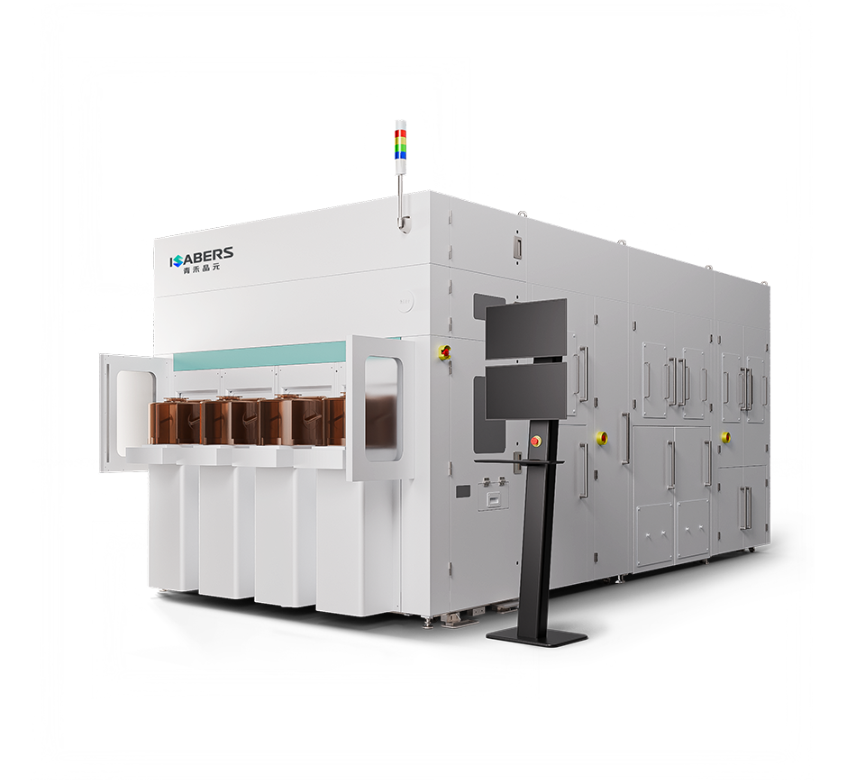
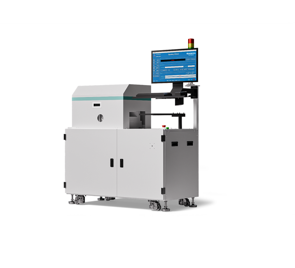
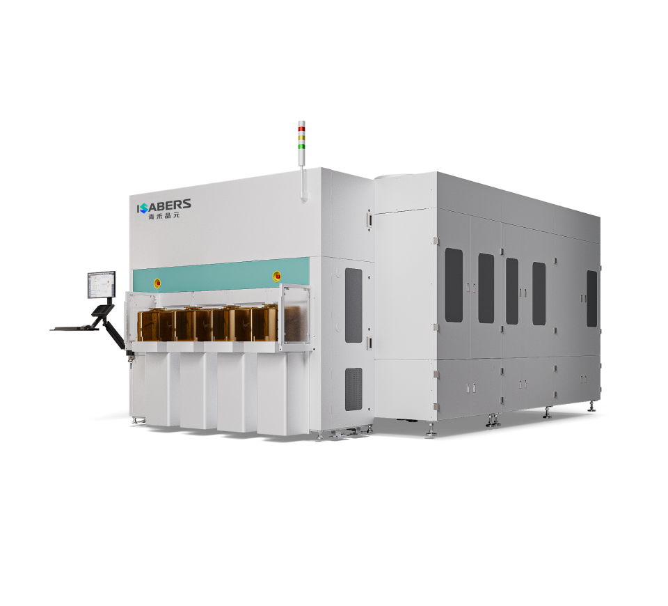
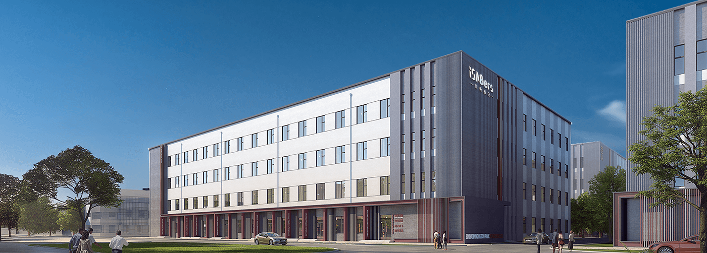
iSABers Semiconductor Technology (Group) Co., Ltd. is a high-tech enterprise specializing in semiconductor bonding integration technology in China. Its core business covers R&D and manufacturing of high-end bonding equipment and precision bonding process foundry services, with technologies widely applied in cutting-edge fields such as advanced packaging, semiconductor device manufacturing, wafer-level heterogeneous material integration, and MEMS sensors. Through its dual-driven model of "equipment manufacturing + process services," the company has established full-industry-chain solutions and successfully developed four independent intellectual property product portfolios:Ultra-high vacuum room-temperature bonding systems, Hybrid bonding equipment,Thermocompression bonding equipment, Supporting process services."
iSABers sincerely invites you to visit Booth N2-2235 at the SEMICON Shanghai New International Expo Center to collaborate on industrial development.
-
Latest News
- 2025-05-01
- Pay tribute to the strivers in the semiconductor industry and wish you a happy May Day!
-
Latest News
- 2025-04-21
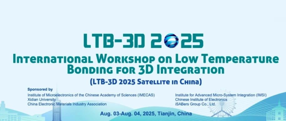
- iSABers Co-hosted – 2025 China International Seminar on Low-Temperature Bonding and 3D Integration Technology Invites You to Participate
-
Latest News
- 2025-03-28
- iSABers SEMICON Moment: Offline Innovation Sharing Session Successfully Held
-
Latest News
- 2025-03-27
- iSABers' SEMICON Moment: Showcasing China's Solutions for Advanced Bonding Technology
-
Latest News
- 2025-03-21
- SEMICON In-Person Advanced Bonding Technology Breakthroughs Symposium