


Core Advantages
-


- Full-Process Technology Platform
- Core bonding technologies: Ultra-high vacuum RT bonding, thermo-compression anodic bonding, temporary bonding, and formic acid-activated bonding—supporting advanced packaging, power modules, and MEMS sensors.
-


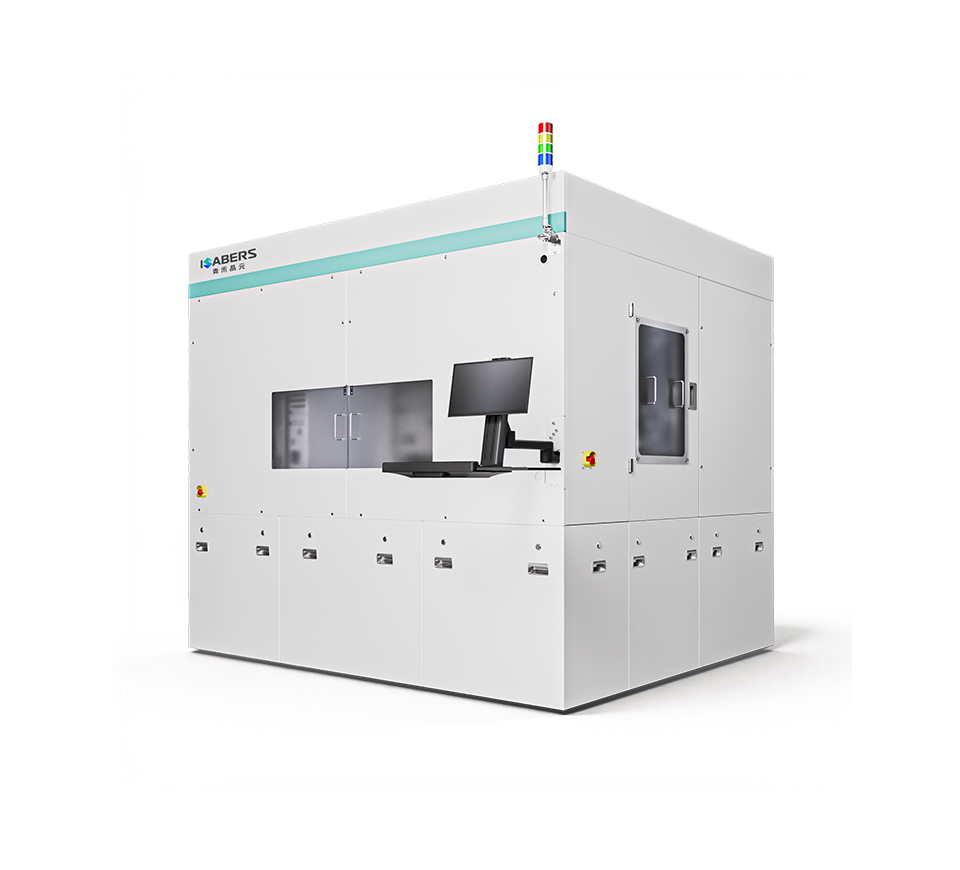
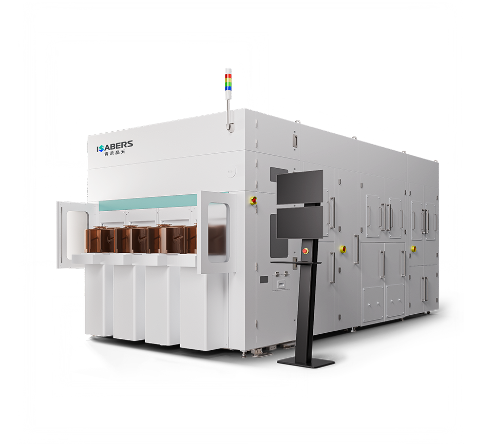
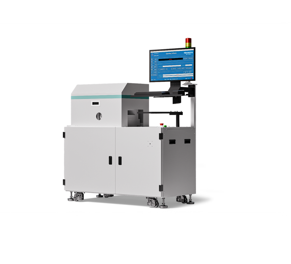
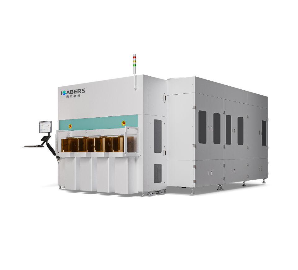
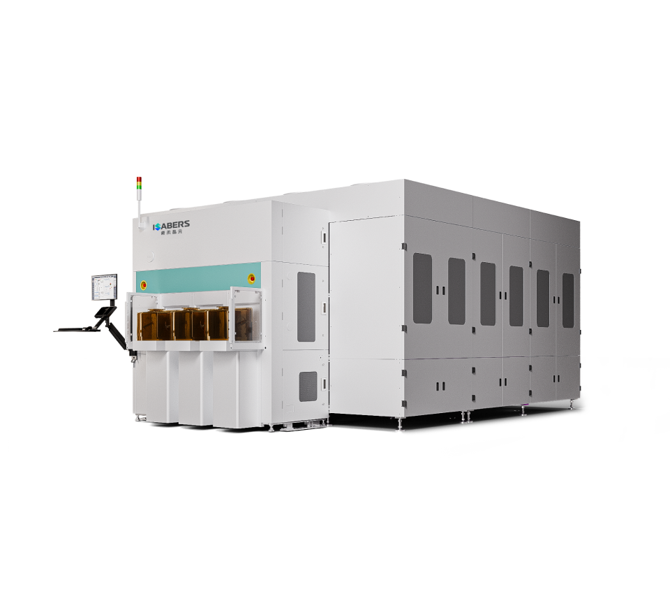
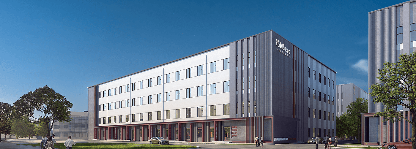
- Top-tier Equipment & Production Capacity
- Equipped with 100+ internationally advanced tools across 2,000㎡ total space, including 2,000㎡ of Class 10/100 cleanrooms. Annual capacity exceeds 60,000 wafers, supporting rapid prototyping and mid-volume production.
-


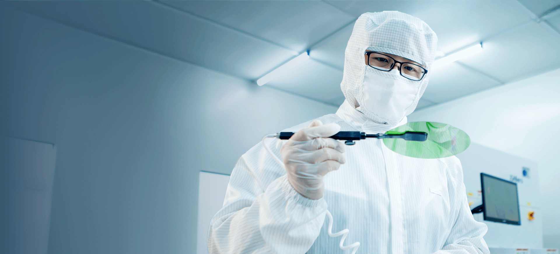
- Expert Team & Quality Assurance
- 50+ senior engineers in our core process teams, each with over 10 years' experience. Strict compliance with international quality standards, including ISO 9001, IATF 16949, ISO 14001, and ISO 45001.
Accreditations

Application Cases