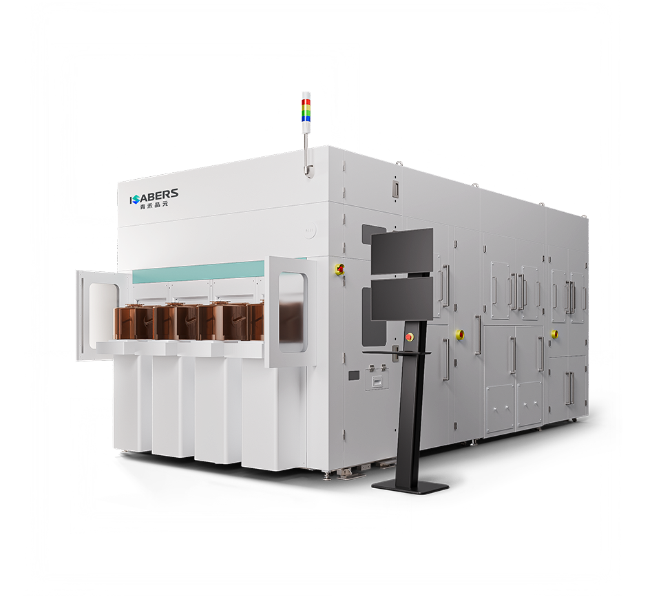
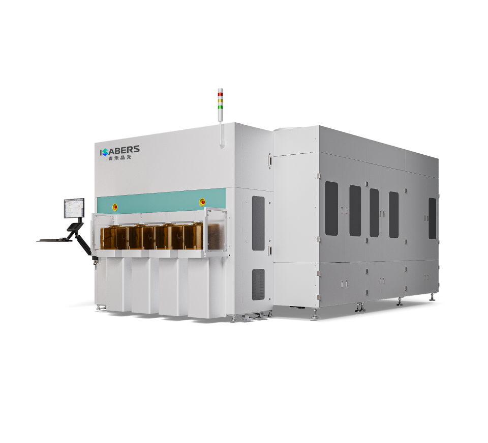
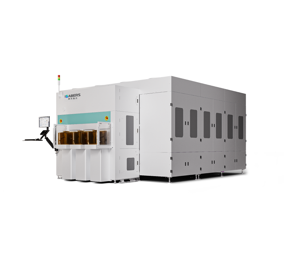


Features
-

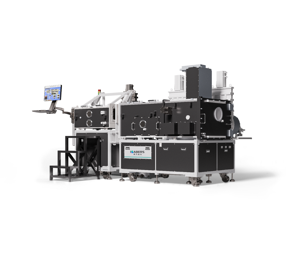
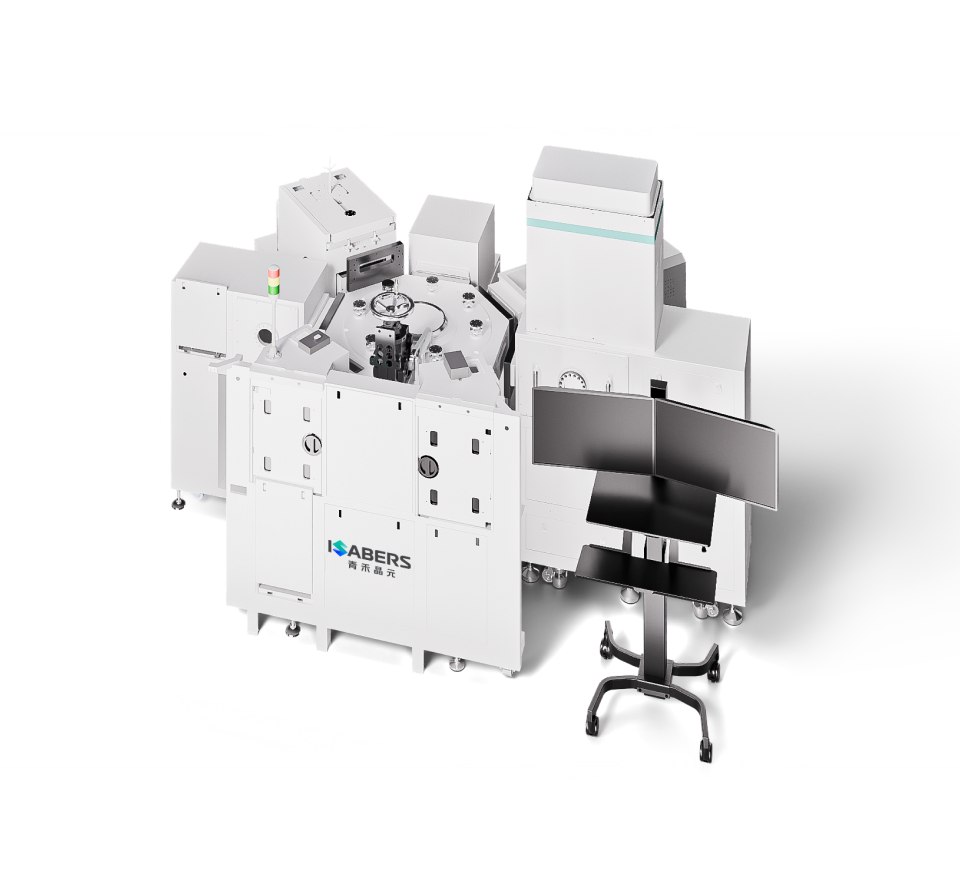
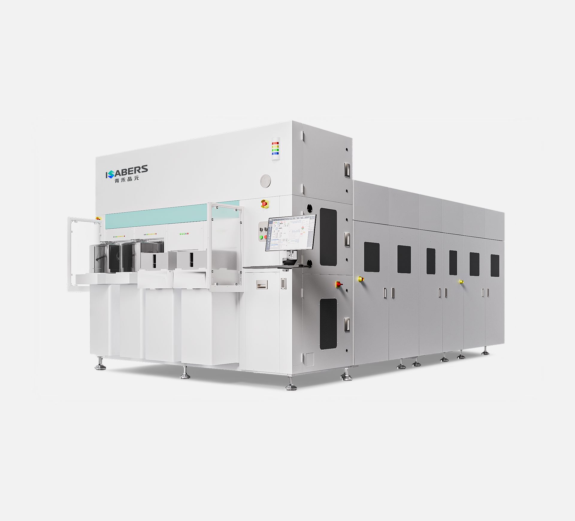
- Dual-Mode Process Integration
- A highly flexible modular design combines C2W and W2W hybrid bonding.
-

- 30% Reduction in Investment Cost
- Integrated architecture eliminates redundant modules compared to separately purchasing C2W and W2W systems.
-

- 60% Reduction in Footprint
- Compact design minimizes floor space compared to separately purchasing C2W and W2W systems.
-

- Enhanced Module Utilization
- Plasma activation and cleaning modules can be used for W2W bonding during C2W bonding operations, eliminating idle time and maximizing efficiency.
Specifications
-
ItemsSpecification
-
Wafer size8, 12 inch
-
Chip size5*8 mm—32*32 mm
1*1 mm—32*32 mm -
W2W Bonding accuracy≤±100 nm
-
W2W Maximum bonding force5N
-
W2W Capacity≥12 pairs/h
-
C2W Bonding accuracy≤±500nm@inter-chip coaxial alignment
≤±200nm@Infrared transmissive alignment -
C2W Maximum bonding force30N
-
C2W CapacitySingle bonding head: >800@200nm@3σ
Single bonding head: >400@50nm@3σ -
Pressure control accuracy±0.5N
-
Pressure control resolution±0.1N