


-
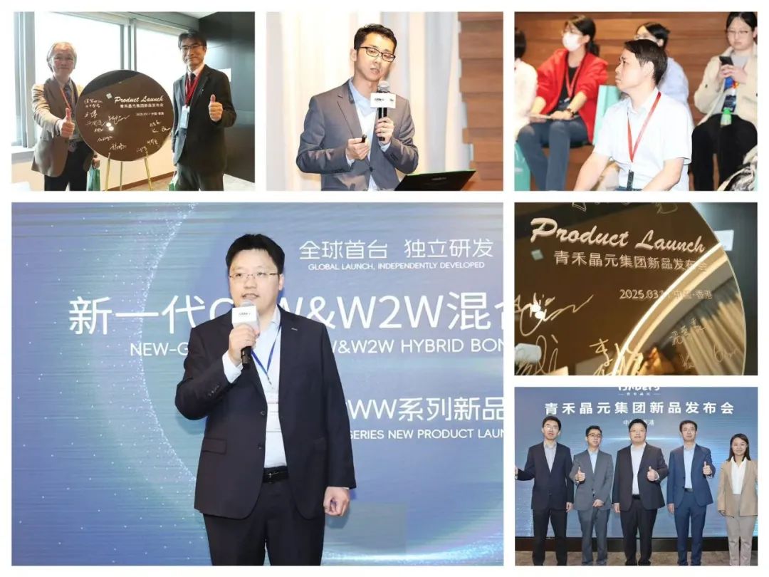
集团资讯2025-03-11
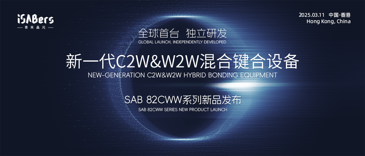
- 【Groundbreaking Launch】iSABers Global Premiere of C2W&W2W Dual-Mode Hybrid Bonding Equipment Redefines Advanced Packaging Benchmark!


【Live from the Launch Event】
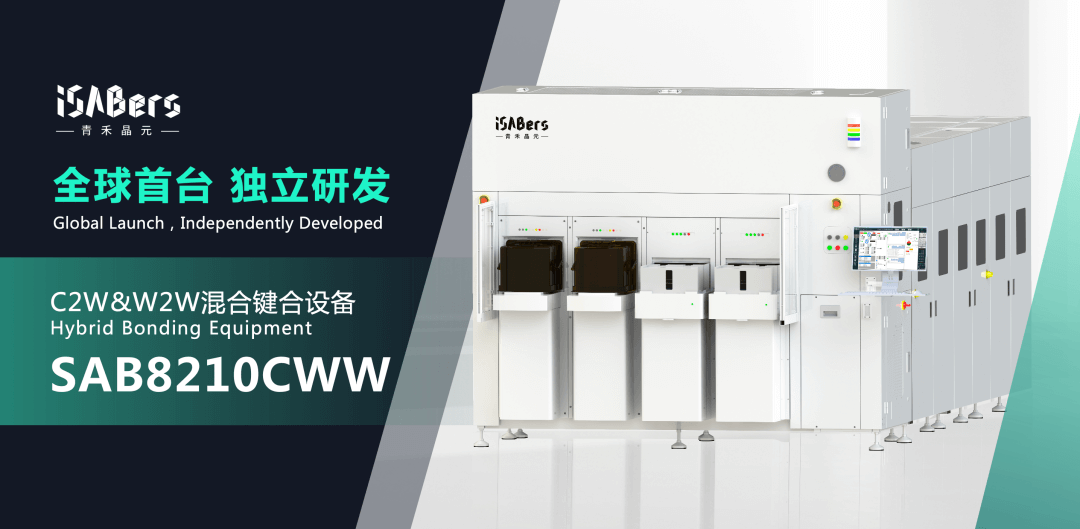
Global First, Independently Developed! iSABers Usher in a New Era of Advanced Bonding Technology
【Breaking Through Moore's Law】
3D Integration Technology: Reshaping the Future of Chips
【Dual-Mode Parallelism: Breaking Boundaries】
【Technological Leadership: Driving Industry Bonding Innovation】
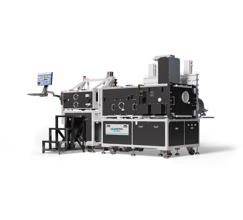
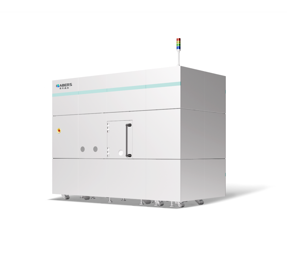
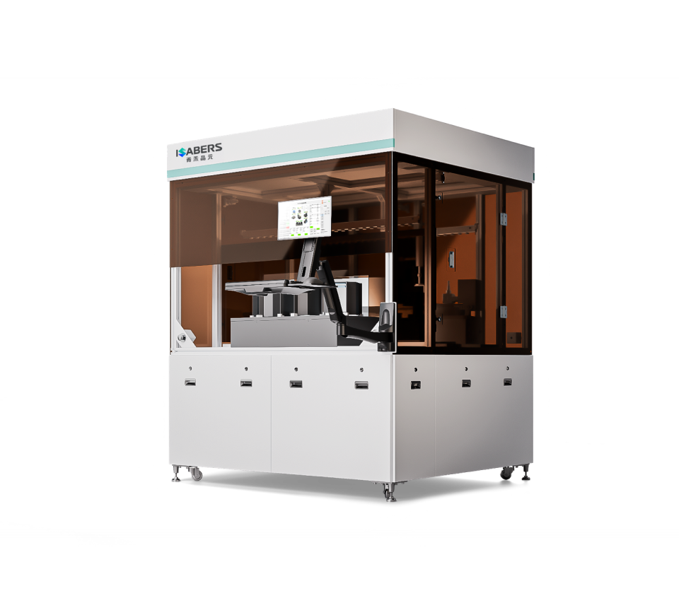
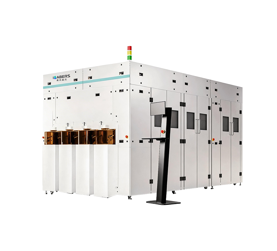
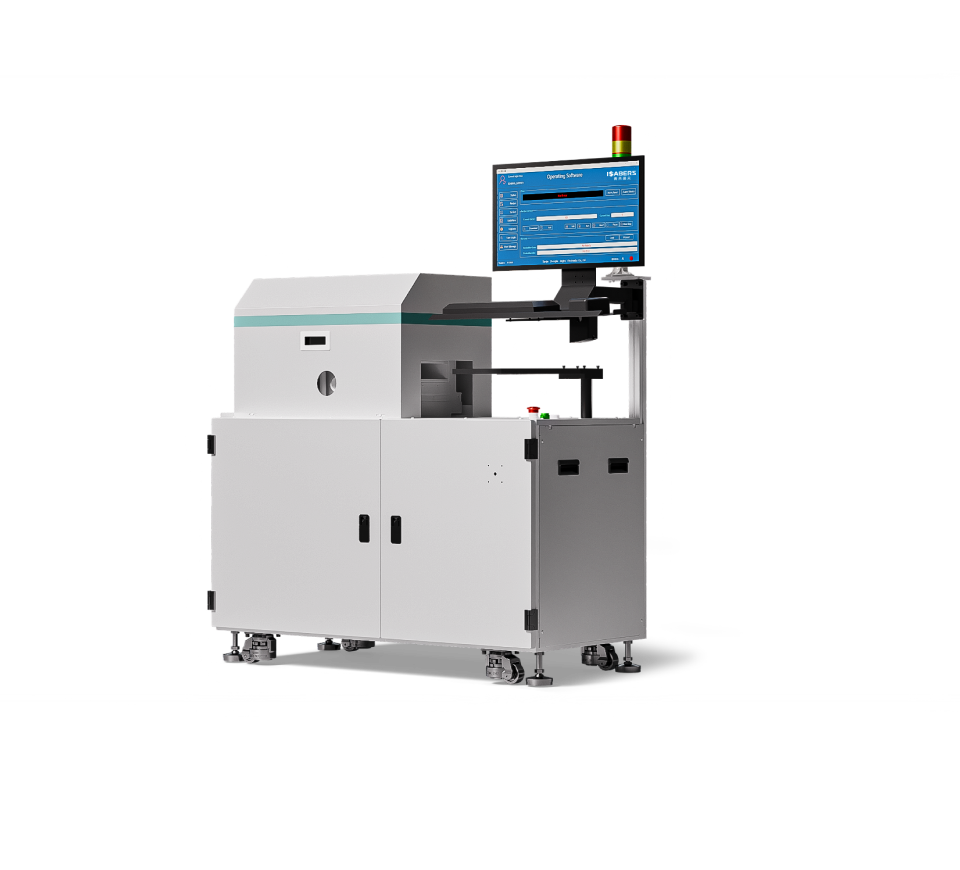
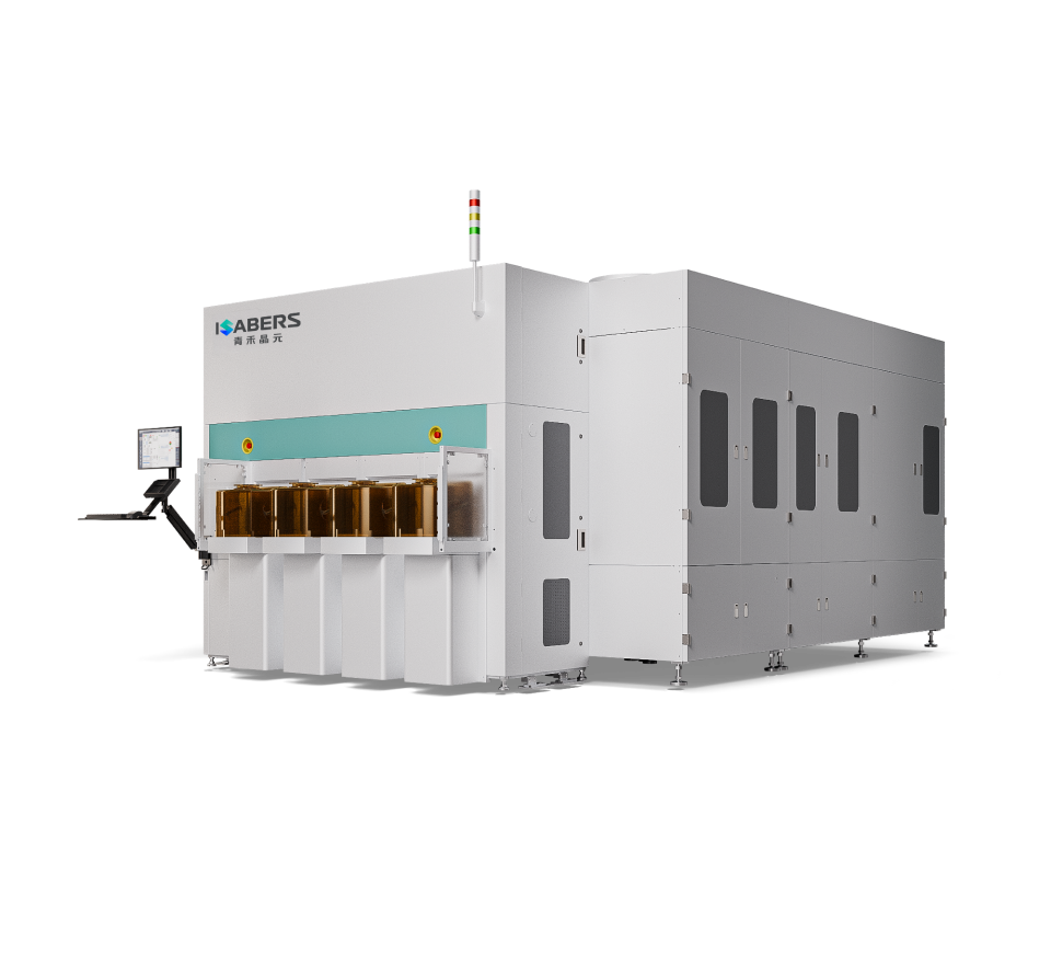
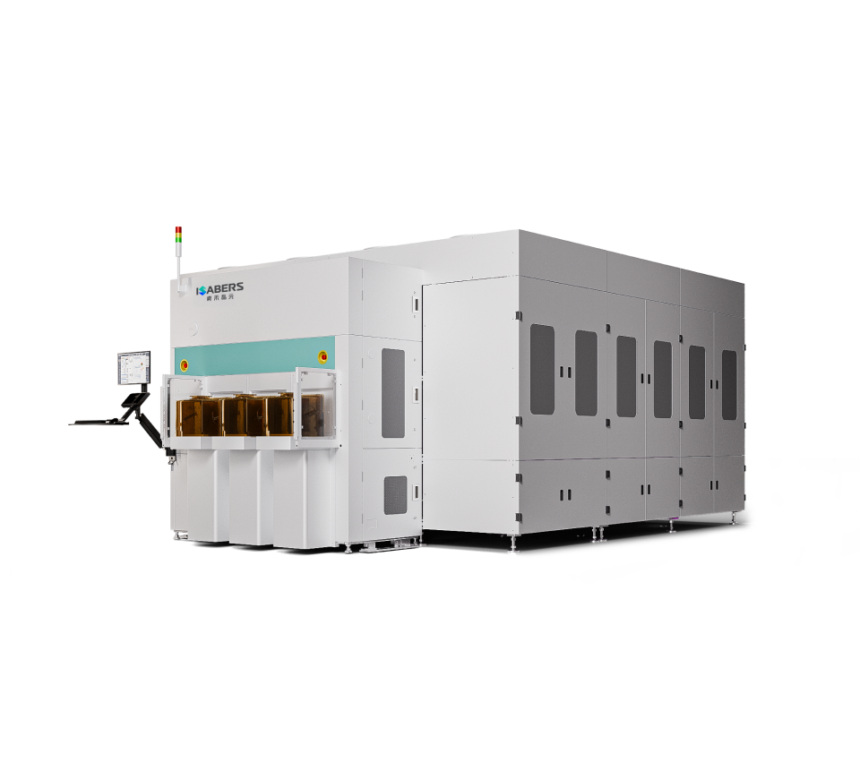
The SAB 82CWW Series hybrid bonding equipment boasts multiple technical highlights:
Dual-Mode Process Integration: Highly flexible modular design supports C2W and W2W dual-mode hybrid bonding, enabling seamless adaptation to R&D and production needs while improving equipment utilization.
Multi-Size Compatibility: Compatible with 8-inch and 12-inch wafers, with quick component replacement for flexibility across different wafer sizes.
Ultra-Thin Chip Handling Capability: Processes chips as thin as 35μm, with full-size compatibility from 0.5×0.5mm to 50×50mm, ensuring production yield and reliability.
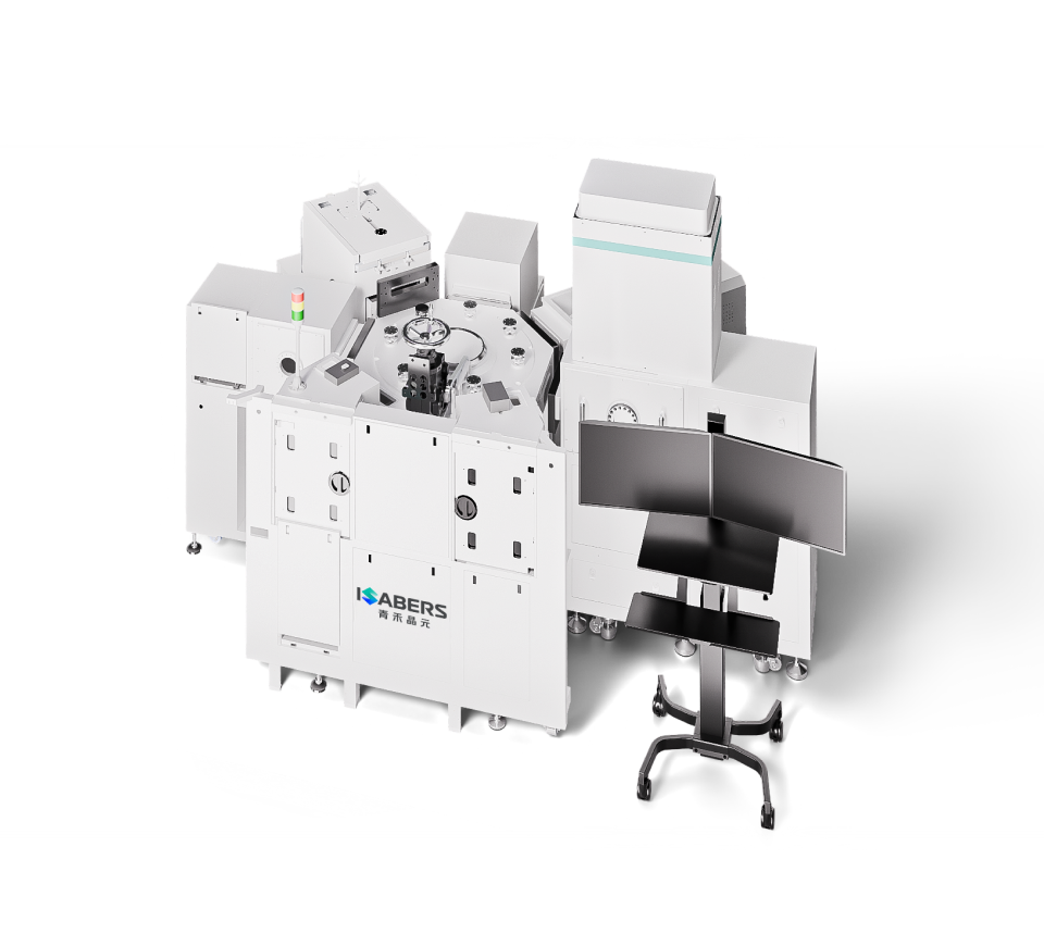
Diverse Alignment Methods: Offers inter-chip coaxial (alignment accuracy >±300nm) and infrared penetration (±100nm) alignment, suitable for chips of varying sizes and materials.
Innovative Bonding Approach: Minimizes particle contamination risks through bonding method innovations, achieving high-yield bonding.
High Precision & Efficiency: C2W and W2W bonding achieve ±30nm alignment accuracy and ±100nm bonding precision, with C2W single-bondhead UPH reaching up to 1,000 chips/hour.
Intelligent Offset Compensation: Equipped with high-precision, high-throughput detection modules and built-in algorithms for negative feedback offset compensation, ensuring bonding precision stability.
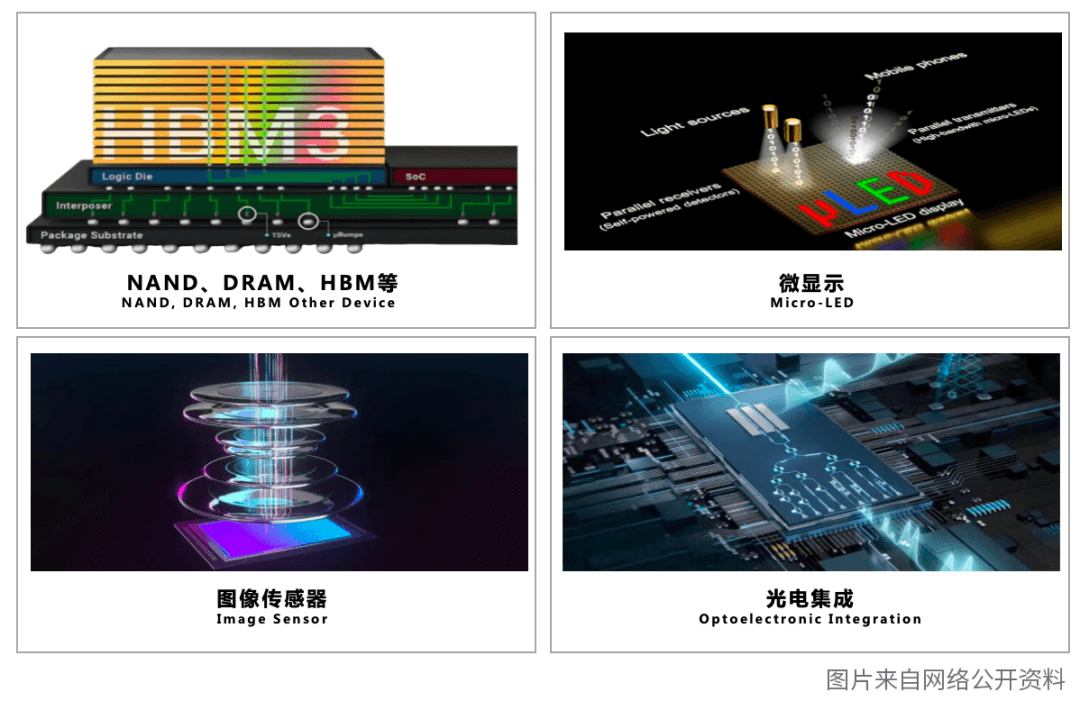
【Empowering Multi-Industry Applications: Driving Innovation】
The SAB 82CWW Series hybrid bonding equipment demonstrates broad application prospects in memory, Micro-LED displays, CMOS image sensors, optoelectronic integration, and other fields. iSABers will continue to deepen its focus on advanced packaging technology, using the SAB 82CWW Series as a starting point to invest in R&D and launch more customer-centric products. Together with global partners, the company aims to push semiconductor heterogeneous integration technology to new heights.
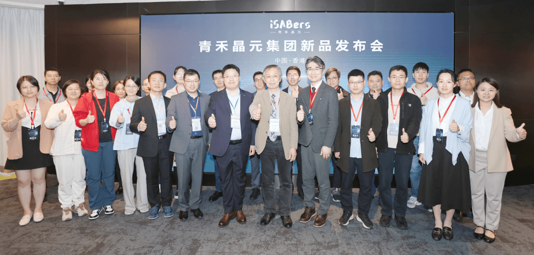
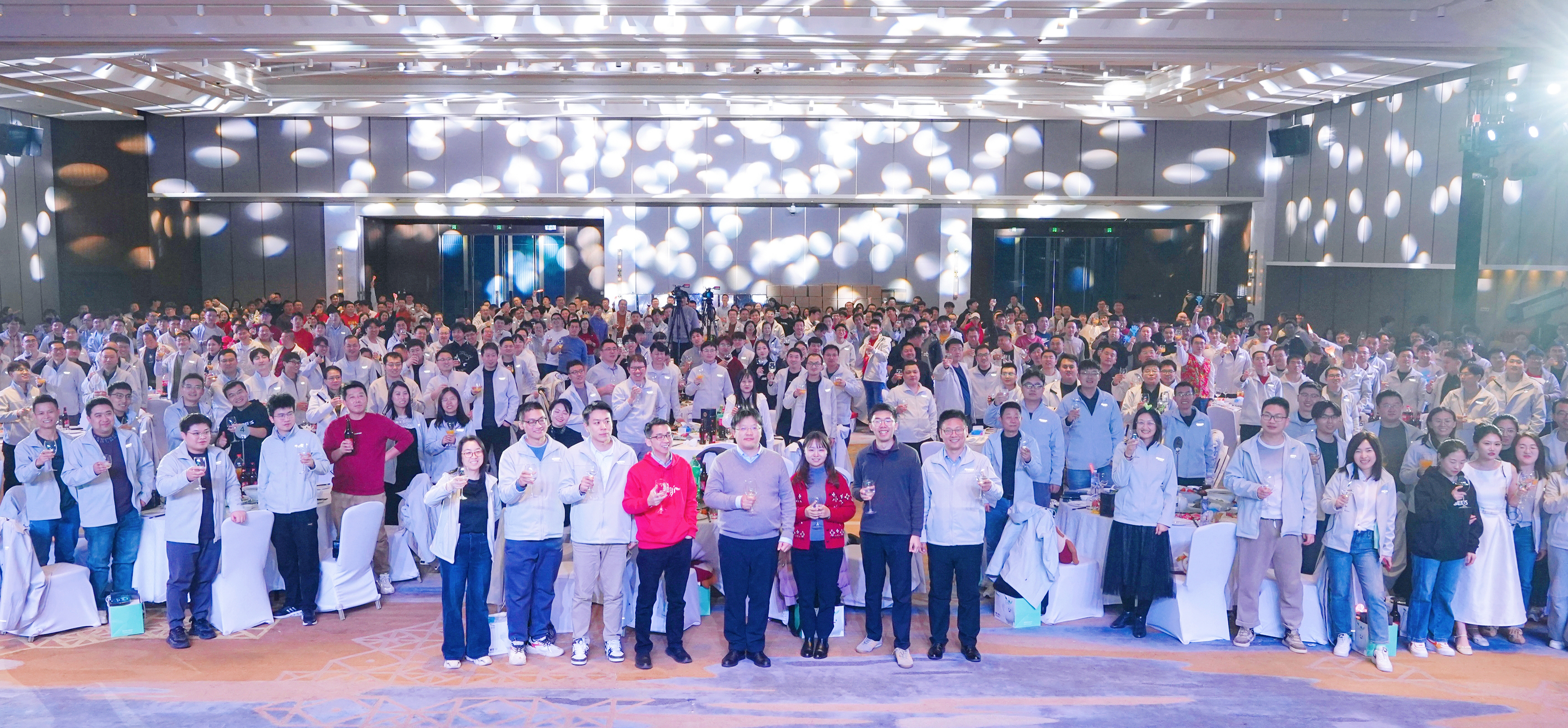
Group Photo of Attendees