


-
集团资讯2024-12-20
- iSABers News | iSABers Collaborates with Partners to Unveil Latest Technological Breakthrough at the 'Olympics' of Semiconductor Devices - IEDM 2024!


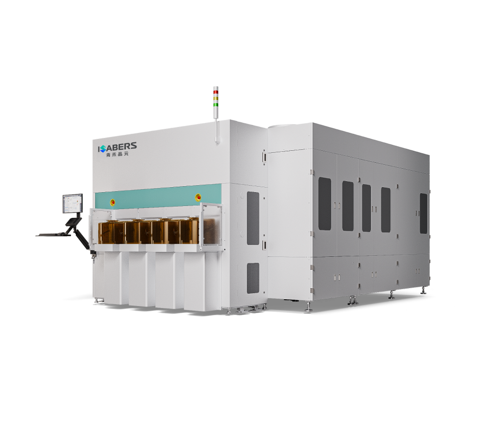
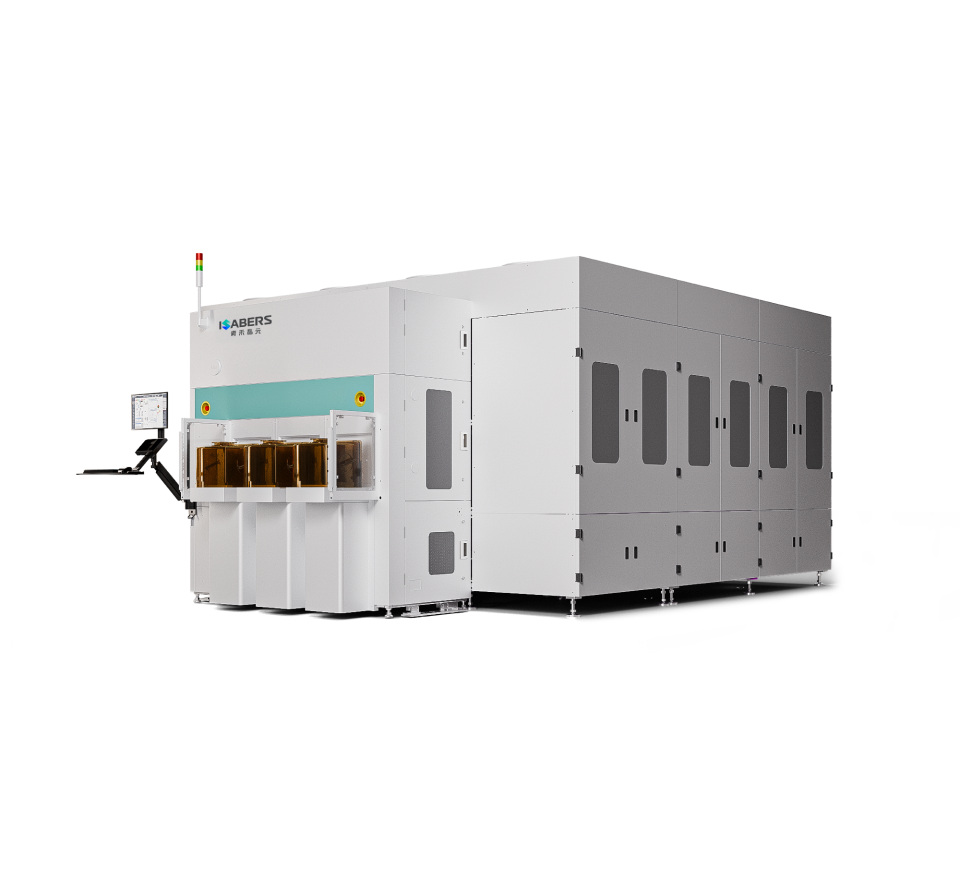
Recently, iSABers Corporation, in deep collaboration with the High-Frequency and High-Voltage Center of the Institute of Microelectronics of the Chinese Academy of Sciences (CAS) and the Nanjing Electronic Devices Institute, successfully developed a high-performance and low-cost 1200V SiC MOSFET based on 6-inch Emerald-SiC composite substrates. The research findings were presented as an oral report at the 70th International Electron Devices Meeting (IEDM 2024) on December 10 in the paper titled "Cost-Effective 1200 V SiC MOSFETs on a Novel 150 mm SiC Engineered Substrate with Dummy Grade Material Reuse", with Dr. Mu Fengwen of iSABers serving as a co-corresponding author.
Current Industry Challenges: The silicon carbide (SiC) wafer industry is rapidly expanding production to meet growing market demands. However, the yield rate of defect-free substrates ("high-quality" substrates) suitable for MOSFET manufacturing typically ranges only from 40%-60%. During the growth and purification of 6-8 inch SiC, low-grade substrates ("low-quality" substrates) are inevitably generated. In current industrial production, these substrates are often discarded as scrap or used as dummy wafers, leading to high production costs for high-quality SiC substrates, which typically account for over 50% of the final MOSFET device cost. Additionally, the energy-intensive manufacturing process of SiC substrates results in high carbon emissions.
Innovative Solution by iSABers and Partners:To address these challenges, iSABers, together with CAS Institute of Microelectronics and other collaborators, internationally pioneered a novel 6-inch single-crystal SiC composite substrate. Through surface-activated bonding technology and ion implantation lift-off techniques, a high-quality SiC thin layer is bonded and transferred onto low-quality single-crystal SiC substrates. This enables effective reuse of low-quality substrates, with each high-quality SiC wafer capable of being recycled over 30 times (i.e., producing over 30 thin layers per wafer), projected to reduce costs by 40%.
iSABers will continue to deepen its expertise in the field of heterogeneous integration technologies, remain committed to providing customers with more efficient and reliable solutions, and drive the sustained progress and development of the entire industry.
The International Electron Devices Meeting (IEDM), founded in 1955, has been dedicated to driving innovation and development in semiconductor devices and related technologies. Hailed as the "Olympics" of the semiconductor device field, IEDM convenes experts and scholars from global top universities, research institutions, and leading enterprises to jointly discuss and showcase cutting-edge research achievements and technological trends. Held annually, this conference is widely recognized as a top academic event of great authority and academic excellence in the field of integrated circuits. Every year, the IEDM event becomes the focus of attention for the global semiconductor industry.
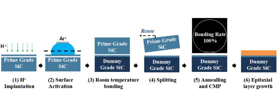
Figure 1.6 Main steps of SiC SiC bonding manufacturing process in 1.6 inches
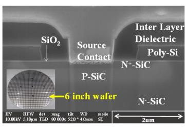
Figure 2. Cross sectional high-resolution transmission electron microscopy (HRTEM) image of the channel region of SiC MOSFET fabricated on 6-inch engineering substrate and epitaxial layer
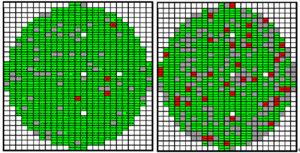
Figure 3. IGSS distribution map of devices fabricated on 6-inch wafers under VGS=-4V and VDS=1200V conditions (green indicates pass through, with a yield of 90% in Figure a and 70% in Figure b)
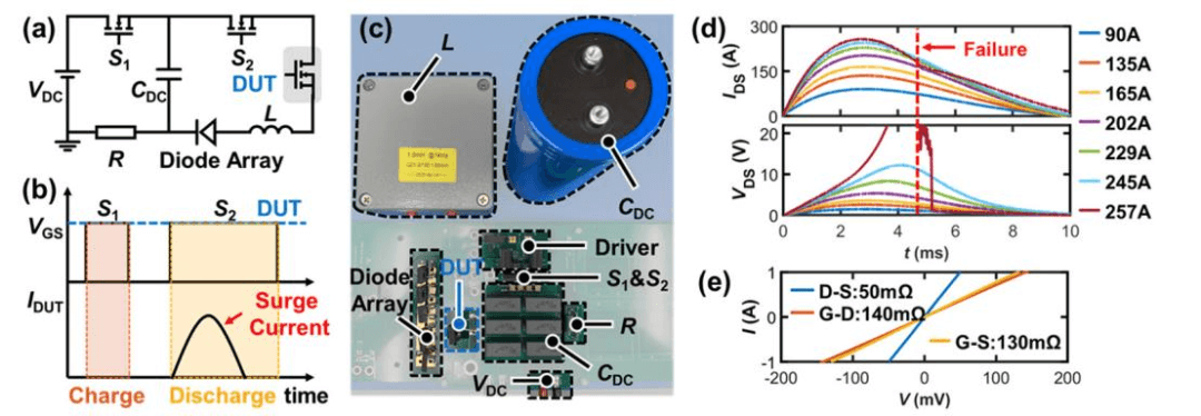
Figure 4. Surge Circuit Test Diagram
(a) Is it a circuit schematic? (b) It's an ideal waveform
(c) Photo of surge current testing device
(d) To measure the current and voltage waveforms of the tested component at different surge current levels
(e) Pin to pin resistance of the failed tested component