


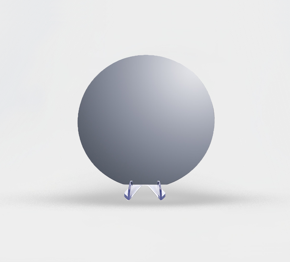
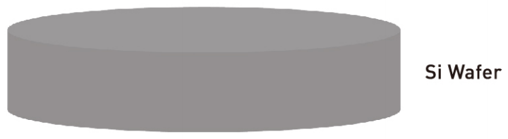
Si Substrate (TTV≤0.5μm)
- Items
- Specification
- Diameter
- 150±0.2 mm
- Si Orientation
- <100>, <110>, <111>, etc.
- Si Type
- P/N
- TTV
- ≤0.5 μm
- Front roughness
- Ra≤0.2 nm (5 μm * 5 μm)
- Items
- Specification
- Diameter
- 200±0.2 mm
- Sl Orientation
- <100>, <110>, <111>, etc.
- Si Type
- P/N
- TTV
- ≤0.5 μm
- Front roughness
- Ra≤0.2 nm (5 μm * 5 μm)