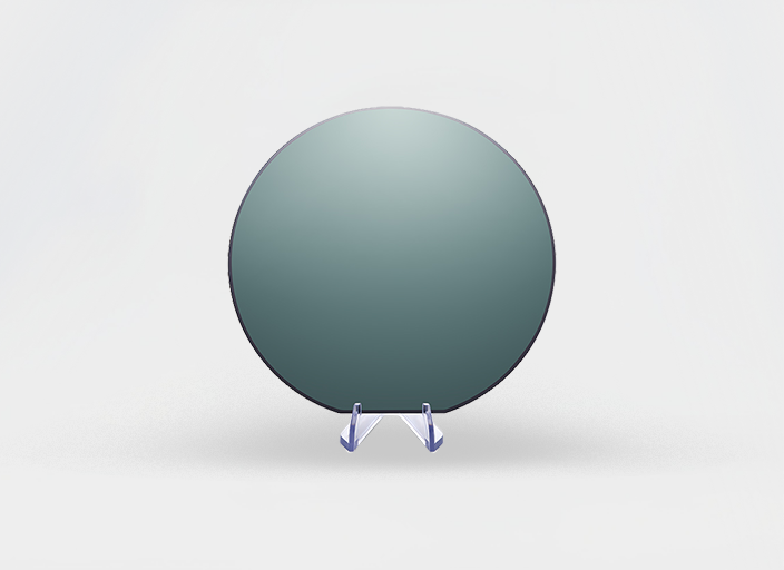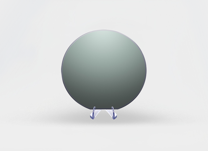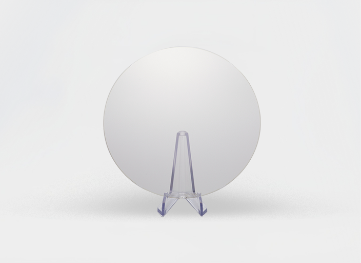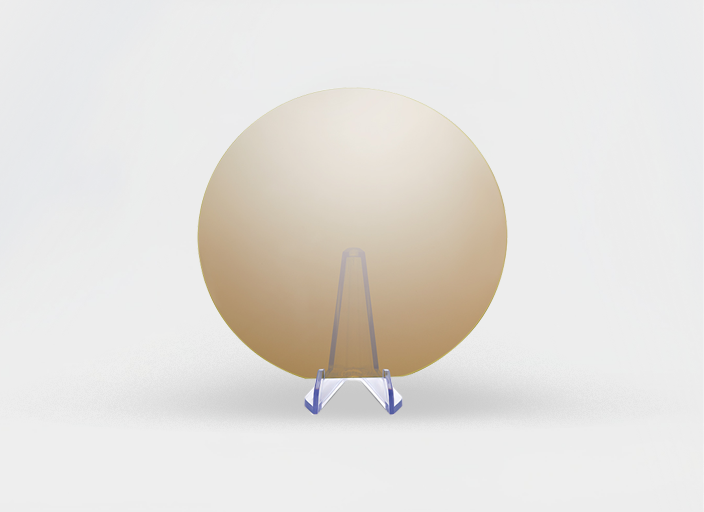

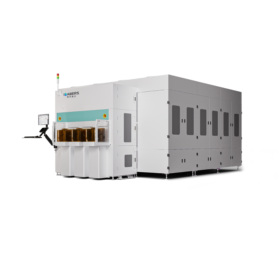


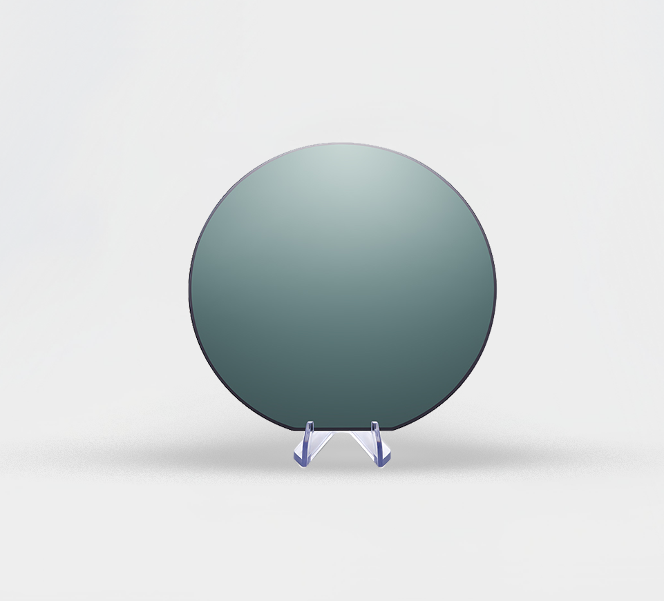
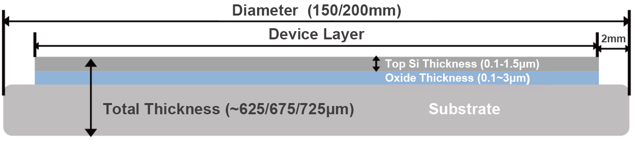
H-Cut SOI Substrate
- Items
- Specification
- Diameter
- 150/200 ± 0.2 mm
- SI Orientation
- <100>, <110>, <111>, etc.
- Dopant Type
- P/N
- Device layer Si Thickness
- (0.1 ~ 1.5 μm) ± 20 nm
- Edge Chip, Scratch, Crack (visual inspection)
- None
- Front roughness
- Ra ≤ 0.2 nm (5 μm * 5 μm)
- BOX layer thickness
- 0.02 ~ 3 μm
- TTV
- ≤5 μm
- BOW
- -40 ~ 40 μm
- Warp
- ≤50 μm
- Total Thickness
- 625 / 675 /725 ± 25 μm